

nanosystec
Booth number: A123
www.nanosystec.com
About us
Headquartered in Germany, nanosystec addresses customers worldwide – with more than 25 years experience in designing and building high precision alignment and assembly stations as well as optical/electrical characterization systems.
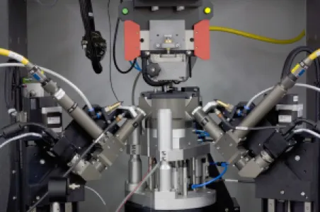
The NanoGlue, NanoWelder and NanoSolder Stations are partly or fully automated production stations for demanding alignment and low-shift assembly procedures in the opto-electronics industry, both for production and product development. The linear axes work with 5 nm resolution, angular rotation resolution is below 0.001°. Long travel ranges facilitate the loading and unloading procedures while the modular architecture allows for fast and reliable customization.
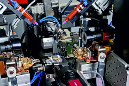
The VersaSeries mounts opto-electronic assemblies and other precision devices with a precision between 1 µm and 10 µm. Typical processes include the placement of laser structures, optics, apertures and similar components requiring high accuracy. The assembly techniques include gluing and UV curing, selective laser soldering and hot bar soldering, eutectic bonding and laser welding. These stations often replace tedious manual assembly procedures.
NanoTest performs optical and electrical characterization for Silicon Photonics Devices on wafer and chip level, VCSEL wafers, laser bars and CoS and High-Density PICs. The graphic interface displays panels for system functions, such LIV curves, OSA measurement and S factors of the network measurements.
Applies for all nanosystec systems: According to the production volume, loading is performed manually or automated with robots, belts and feeders. All stations can be customized to perfectly reach the desired technical performance and throughput. The TestMaster software package with advanced machine vision algorithms allows for unattended operation while providing high yield.


Address
Marie-Curie-Strasse 6
64823 Gross-Umstadt
Germany
E-mail: sales@nanosystec.com
Phone: +49 6078 782540
Internet: www.nanosystec.com
Contact person:
Sales Manager Guenter Hummelt
E-mail: sales@nanosystec.com
Phone: +49 6078 782540
NanoSeries Alignment and Assembly Stations
The NanoGlue, NanoWelder and NanoSolder series are partly or fully automated production stations for demanding alignment and low-shift assembly procedures in the opto-electronics industry. Nanosystec offers standard and custom configurations.
The linear axes work with 5 nm resolution, angular rotation resolution is below 0.001°. Long travel ranges facilitate the loading and unloading procedures while the modular architecture allows for fast and reliable customization.
A powerful process software with automated machine vision algorithms allows for unattended operation with high yield.


VersaSeries Precison Placment Stations
The semi or fully automated production of the VersaSeries are used for complex assemblies which require precision in the low micrometer regime. Assembly techniques include micro welding, selective soldering by laser or hotbar and gluing (with subsequent UV or thermal curing) plus laser fine cutting.
The motion system consists of high-precision linear and rotary stages to offer adjustment capability in all degrees of freedom. The gantry configuration provides superior repeatability over the entire work surface.
Various processing methods can be combined in one station. Feeders, belts and robots facilitate full automation while exchangeable grippers offer highest versatility.


NanoTest Optical and Electrical Characterization Stations
NanoTest performs optical and electrical characterization for Silicon Photonics Devices on wafer and chip level, VCSEL wafers, laser bars and CoS and High-Density PICs.
All NanoTest stations combine precise measurements with high speed, proven reliability and ease of use. The versatility qualifies the stations not only for high volume quality assurance, but also for demanding development applications.
The graphic interface displays panels for system functions, such LIV curves, OSA measurement and S factors of the network measurements.
All measured data can be stored in a local database or transferred into the customer’s system.


